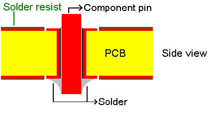
Through hole pin
In the above figure a through hole pin is shown.
After soldering this through hole pin will look like
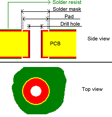
After the bottom side of the PCB has gone through a solder bath, all copper areas at the bottom of the PCB are soldered. The copper areas on the bottom PCB side which are covered with solder resist, are not soldered.
Usually the anti pad for the solder mask is 8 mil greater than the copper pad. The size of +8 mil for the solder mask, is because of tolerances.